
Printed Circuit Boards (PCBs) are the backbone of modern electronics. They are the physical platform that connects and supports electronic components, allowing devices to function efficiently. Whether you’re a hobbyist building your first electronic project or a seasoned engineer designing a complex electronic system, understanding PCB design is essential. This step-by-step guide will walk you through the fundamental PCB design process.
- Define Your Project Requirements
The first step in PCB design is to define the project’s requirements. What is the purpose of the PCB, and what specific components will it include? Consider factors such as size, power requirements, signal integrity, and the environment in which the PCB will operate. These initial specifications will guide the rest of the PCB design tools process.
- Schematic Capture
Create a schematic diagram that represents your circuit’s electronic connections and functions. You can use specialized software like Eagle, KiCad, or Altium Designer. Place symbols for components and connect them with lines representing wires or traces.
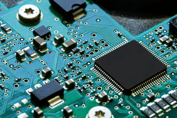
- Component Selection
Select the electronic components needed for your project, such as resistors, capacitors, integrated circuits, and connectors. Consider factors like component availability, cost, and performance. Once chosen, you’ll need to find or create component footprints representing how the components will physically fit on the PCB.
- PCB Layout
With the schematic as a guide, move on to the PCB layout stage. In this step, you’ll arrange the components on a virtual board, placing them in their physical positions and connecting them with traces. Consider factors like component placement, signal routing, and heat dissipation. Ensure that components are not too close to each other and that you have enough space for traces.
- Trace Routing
Routing traces involves drawing the copper pathways that connect the various components. When routing traces, consider the path of least resistance and minimize the length of high-speed signal traces to reduce signal degradation. To ensure signal integrity, follow good design practices, such as maintaining proper clearance between traces and avoiding sharp angles.
- Power and Ground Planes
For many PCBs, it’s essential to have power and ground planes to provide a stable voltage reference and reduce electromagnetic interference. Place power and ground planes on separate layers and use Vias to connect them to the components that need power and ground connections.
- Design Rule Check (DRC)
Before finalizing your design, run a Design Rule Check to ensure your PCB adheres to the manufacturer’s specifications and common design rules. DRC checks for issues like trace width violations, clearance violations, and unconnected nets.
- Gerber File Generation
The Gerber file format is the standard for PCB fabrication. Use PCB design software to generate Gerber files, which contain all the information needed to manufacture your PCB, including layer information, trace patterns, and component placement.
- PCB Fabrication
Submit your Gerber files to a PCB manufacturer. They will produce your PCB based on your design specifications. You can choose from various PCB fabrication options, including materials, layer counts, and finishes.
- Assembly
Once you receive your fabricated PCB, you’ll need to assemble it. This involves soldering the components onto the board. Pay attention to the soldering process, ensuring you don’t overheat or damage components.
- Testing and Debugging
After assembly, it’s crucial to test and debug your PCB. Use multimeters, oscilloscopes, and other test equipment to verify that your circuit functions as expected. If you encounter issues, trace back through your design to identify and correct the problems.
- Documentation
Proper documentation is essential for future reference and troubleshooting. Document your PCB design, including the schematic, bill of materials, and any unique design considerations. This information will be invaluable for maintenance, repairs, and future project iterations.